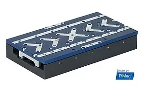
PI’s optimization technology has proven to dramatically improve production economics in processes as diverse as photonics wafer probing, device packaging, chip testing, and even laser and optical equipment manufacturing. The combination of blazing speed, nanoscale performance, and industrial robustness reduces costs and improves yield worldwide. Now the flexible combination of PI´s industrial stages and new alignment-enabled controls from ACS addresses additional tough throughput and yield challenges for photonics production.
This conceptual demo shows how PI’s fast alignment can apply to large-area applications such as pick-and-place, and the screening, assembling, and testing of photonic devices. From the wafer, through coupon and chip, to the packaged product. The system performs a rapid localization, scanning, and fast lock-on and tracking of a series of photonic components over a large area.
This opens new possibilities for hyper-efficient systems architectures in large-format production processes. PI’s unique optimization functionality is firmware-based, offers parallel alignment across multiple inputs, outputs, and degrees-of-freedom, and can improve process throughput by a factor of 100 or more compared to legacy approaches.
The Study Integrates:


PI´s fifth-generation fast alignment technology combined with the open-architecture modular controls from ACS enables the flexible construction of sophisticated systems, providing extraordinary performance with advanced safety provisions. These functionalities provide especially rapid throughput with seamless compatibility with today’s photonic devices, which often prove challenging for legacy technologies.