Product and System Demonstrators High-Precision Laser Processing for Wafer Dicing

High-Precision Laser Processing for Wafer Dicing

High Guiding Accuracy – Exceptional Velocity Control – High Repeatability

Manufacturing chips and microchips involves cutting the wafers, using a process known as wafer dicing, into small square or rectangular “chips” or “die”. Typical challenges to consider in wafer dicing applications are: To position the cut accurately, to minimize the losses of material, and to minimize distortions of the components. While at the same time, the maximum possible machining speed must be achieved. As the requirements are constantly increasing, laser dicing has become the preferred dicing technology. This noncontact laser process is flexible and avoids flaking at the cutting edges. The good quality of the edges, which is one of the decisive factors for fracture resistance, can be further improved with various automated postprocessing processes. This significantly reduces production waste and, therefore, saves production costs. Accordingly, laser-dicing processes also demand motion systems that offer high accuracy and high straightness at high velocities.


Key Features of the Motion Solution


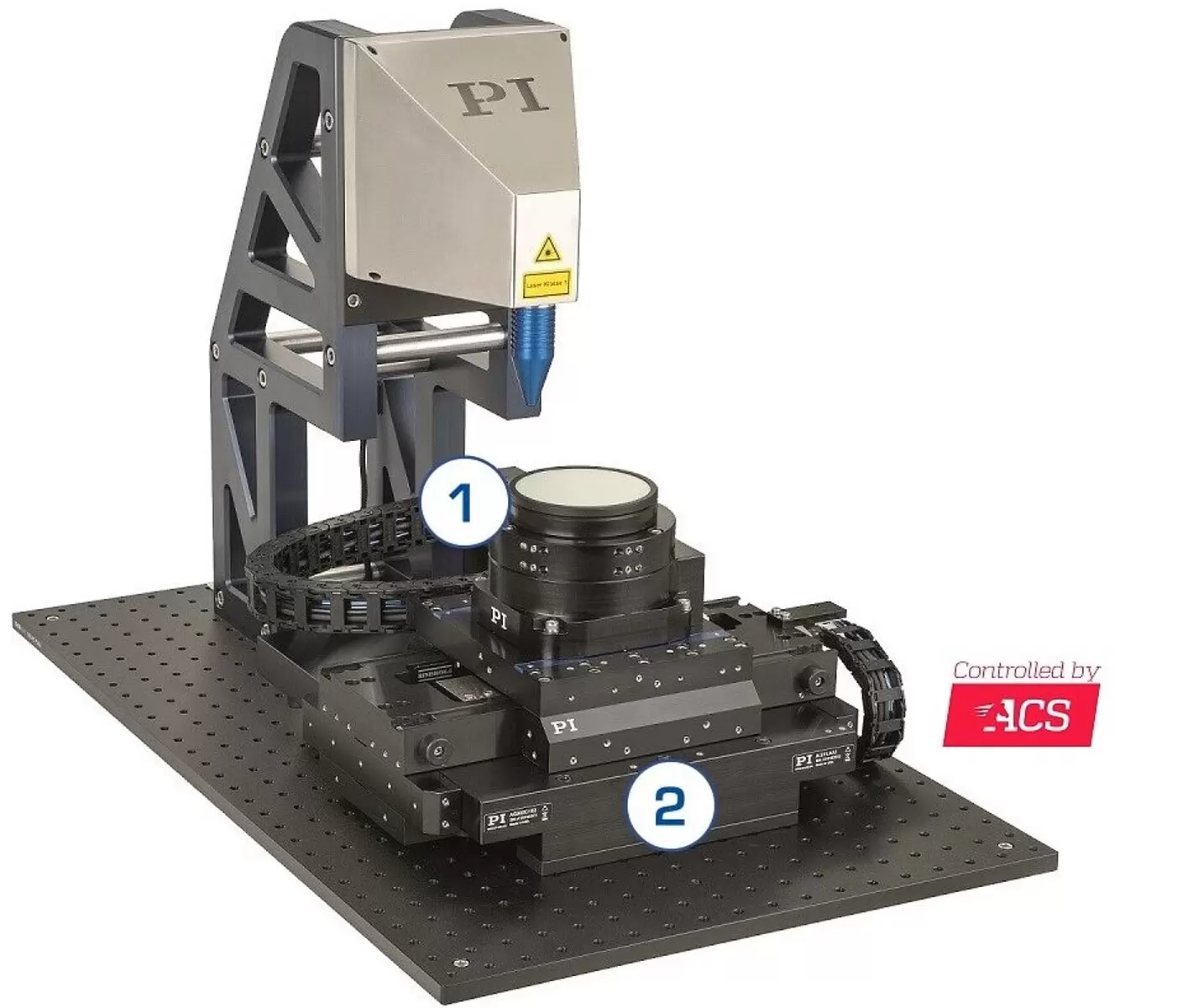
  • Direct-drive linear and rotation stages with air bearings for ultimate precision
  • High straightness, flatness, and repeatability
  • Elimination of cogging for smooth velocity control
  • Drag chain cable management
  • Metrology provided at wafer work point
  • 24/7 operations with high duty cycles
  • Absolute encoders eliminate referencing while increasing efficiency and safety during operation


Rotation Axis - Wafer Orientation and Correction

  • Air bearing rotation stage
  • Direct-drive cogless motion
  • Superior travel accuracy, flatness, and wobble performance
  • High stiffness and load capacity
  • Cleanroom compatible


Scan Axis

  • XY planar air bearing stage
  • High velocities and accelerations
  • Excellent geometric performance
  • Resolution to 1 nm
  • Low profile for limited installation space
  • Cleanroom compatible


Motion Control

  • High performance EtherCAT® motion controller presented in a 19”-rack with integrated drives, power supplies, and functional safety.
  • NanoPWM™ drive technology enables nanometer tracking error and optimal velocity.
  • Advanced servo control algorithms such as


System in Motion


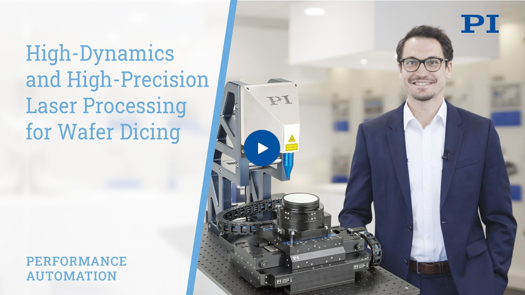
The video shows the advantages of the linear stages for industrial laser micromachining


Further Industries and Applications that Benefit from this Motion Solution

Laser Material Processing: Ultra-Fast Laser Ablation
Electronics Manufacturing: DCB (Direct Copper Bonded) Circuit Board Scribing
Semiconductor: Wafer Scribing and Singulation – Wafer Inspection – Defect Detection
Medical: DNA Luminance Testing – Device Manufacturing
Additive Manufacturing: Twin Photon Polymerization
Direct the future with the power of the past.
Expertise
Markets Technologies
Contact
Nano Dünya Mak. San. Tic. Ltd. Şti.
Parseller Mah. Gündoğan Sok. No:8/A
Ümraniye/İstanbul

02166140039
info@nanodunya.com.tr
Copyright © 2024 by Nano Dünya. All rights reserved.
x
Quote List
Your quote list is currently empty.
x
Download Request
Your download list is currently empty.
0 0 Whatsapp